Fairchild Semiconductor in the Early Silicon Era: Defining the Modern Integrated Circuit
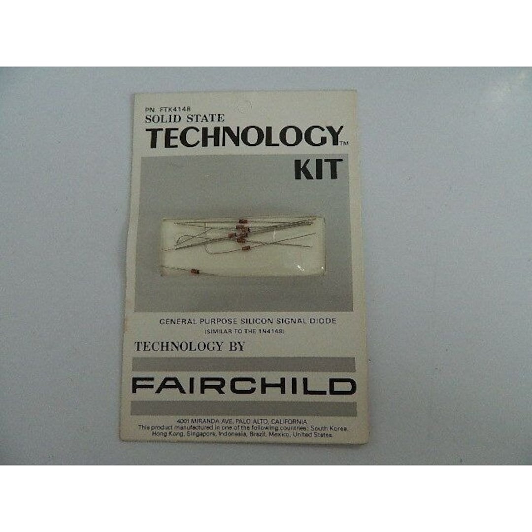
Fairchild Semiconductor’s inception in 1957 and its subsequent innovations in the 1960s fundamentally transformed the electronics industry by transitioning from discrete transistors to the mass production of planar silicon integrated circuits. This period established the technological and business infrastructure of Silicon Valley, driving the scalability, miniaturization, and reliability standards that continue to underpin modern semiconductor manufacturing in 2026.
The Genesis of Fairchild Semiconductor: A Departure from Tradition
The story of Fairchild Semiconductor began as an act of scientific rebellion. In 1957, eight engineers and scientists—later dubbed the "Traitorous Eight"—left Shockley Semiconductor Laboratory. Their departure was fueled by dissatisfaction with the management style of William Shockley and a shared vision regarding the potential of silicon as the base material for semiconductor devices.
Supported by Sherman Fairchild, who provided the initial $1.5 million in capital, the team formed Fairchild Semiconductor in Mountain View, California. At the time, the prevailing industry standard for transistors relied on germanium, a material prone to thermal instability. The founders of Fairchild were convinced that silicon, while more difficult to refine, offered superior performance and heat tolerance, essential for the aerospace and military applications that represented the primary market demand of the era.
The Planar Process: A Technological Turning Point
The most significant contribution of Fairchild Semiconductor during the early silicon era was the development of the planar process in 1959. Before this innovation, transistors were produced using a "mesa" technique, which involved etching away the sides of the silicon crystal to isolate individual components. This method left the sensitive p-n junctions exposed to contaminants, leading to high failure rates and unpredictable performance.
Jean Hoerni, one of the co-founders, pioneered the planar process by using a silicon dioxide layer to protect the junctions. This was not merely a manufacturing refinement; it was a fundamental shift in physics. By using a thermally grown oxide to cover the junction surface during diffusion, Hoerni enabled:
- Improved Reliability: The oxide layer acted as a hermetic seal, preventing impurities from degrading the transistor.
- Mass Production: The process allowed for multiple components to be printed on a single wafer using photolithography, significantly reducing costs.
- Scalability: Planar technology provided a platform for interconnecting multiple components, which directly led to the birth of the integrated circuit.

From Transistors to Integrated Circuits
While the mesa-to-planar transition defined the production of individual transistors, the true revolutionary moment occurred in 1961 when Robert Noyce, another Fairchild founder, filed a patent for the "Semiconductor Device-and-Lead Structure." This invention solved the problem of interconnecting components on a single chip.
Noyce’s integrated circuit (IC) built upon Hoerni’s planar process. By depositing metal leads onto the protective oxide layer, he created a way to connect multiple transistors, resistors, and capacitors on a single monolithic silicon block. This removed the need for manual wire bonding between discrete components, which had been the primary bottleneck in building complex electronic systems.
During the early 1960s, this technology found its first major customer in the United States government. The Apollo Guidance Computer, developed for the NASA lunar missions, was one of the first systems to heavily utilize Fairchild’s ICs. The demand from the space program forced Fairchild to increase manufacturing yields and refine the reliability of their chips, proving that complex computing could be reduced to a size and weight manageable for aerospace applications.
Economic and Industrial Impacts
Fairchild Semiconductor did not just produce hardware; it produced an economic ecosystem. During the 1960s, the company’s internal culture was characterized by a high turnover of talent, which paradoxically turned the company into the "Silicon Valley University." Engineers who gained their foundational expertise at Fairchild frequently left to start their own ventures.
This cycle of spin-offs—including Intel, AMD, and National Semiconductor—created the dense network of venture capital and specialized engineering talent that defines the modern region. The "Fairchild Effect" saw the rapid diffusion of silicon manufacturing expertise, which accelerated the pace of innovation across the entire industry. By 1965, the cost per gate on an integrated circuit began to drop precipitously, enabling the "Silicon Era" to move beyond the laboratory and into commercial calculators, industrial controllers, and eventually, the consumer electronics market.
Comparison of Semiconductor Manufacturing Eras
| Era | Key Material | Component Structure | Primary Market |
|---|---|---|---|
| Pre-Fairchild | Germanium | Point-contact / Mesa | Military / Hearing aids |
| Early Fairchild | Silicon | Planar Transistors | Military / Aerospace |
| Mid-Silicon Era | Silicon | Monolithic Integrated Circuits | NASA / Industrial |
| Late 1960s | Silicon | MOS / LSI Circuits | Computing / Calculators |
Challenges and Limitations in the Early Era
The early silicon era was not without significant obstacles. Manufacturing yields were notoriously low in the early 1960s. A "yield" refers to the percentage of working chips on a single silicon wafer. Because dust, chemical impurities, and crystal defects could ruin an entire batch, companies spent enormous resources on developing cleanroom environments.
Furthermore, thermal management was a constant concern. As engineers packed more transistors into smaller areas, heat dissipation became a limiting factor for performance. Fairchild had to pioneer early packaging techniques, moving from metal "cans" (TO-5 packages) to the ceramic and plastic dual-in-line packages (DIP) that allowed for easier integration onto printed circuit boards.
These technical challenges mandated a shift in management philosophy. Fairchild had to integrate chemistry, physics, and mass-production engineering into a unified workflow. This requirement for cross-disciplinary collaboration is what separated successful semiconductor firms from those that failed to transition from bench-top prototypes to factory-scale production.
Frequently Asked Questions
What made Fairchild’s planar process superior to previous methods? The planar process used a silicon dioxide layer to passivate the surface of the chip. This protected the fragile p-n junctions from atmospheric contamination and provided a base for aluminum interconnects, which made the components significantly more reliable and easier to manufacture in volume.
Why was the Apollo Guidance Computer significant to Fairchild? The Apollo program provided both the funding and the technical requirements to push Fairchild’s integrated circuit production to maturity. NASA’s need for extremely lightweight and reliable computing forced Fairchild to move from artisanal production to standardized manufacturing.
How did the "Traitorous Eight" influence the tech industry? By leaving Shockley and founding Fairchild, they established the model of the high-growth, venture-backed startup. Their alumni went on to found dozens of other companies, creating the "Silicon Valley" model of entrepreneurship and talent mobility.
What was the primary difference between germanium and silicon in the 1960s? Germanium transistors were faster to produce initially but unstable at high temperatures. Silicon, although harder to process, offered greater stability, which allowed for the denser, more complex circuitry required for the integrated circuits that followed.
Did Fairchild invent the first transistor? No. The transistor was invented at Bell Labs in 1947 by Bardeen, Brattain, and Shockley. Fairchild’s contribution was the development of the planar silicon transistor and the monolithic integrated circuit, which allowed the technology to be mass-produced.
Next Steps for Researchers and Enthusiasts
To understand the full impact of Fairchild Semiconductor, researchers should consult the archives of the Computer History Museum in Mountain View, which holds significant documentation on the 1960s manufacturing processes. Those interested in the technical progression should focus on the 1961 patent filings by Robert Noyce, which delineate the transition from discrete wiring to monolithic integration. For a contemporary look at these legacy processes, examine the "Small Scale Integration" (SSI) data sheets from the mid-1960s, which illustrate how simple logic gates were first combined to form complex computational pathways.
Image Gallery
Select an image to open it in a new tab.

Lars Thomsen
Global Labor Markets and Economic Strategy Editor
