Grounding Planes for Electrical Safety: Principles, Design, and Implementation
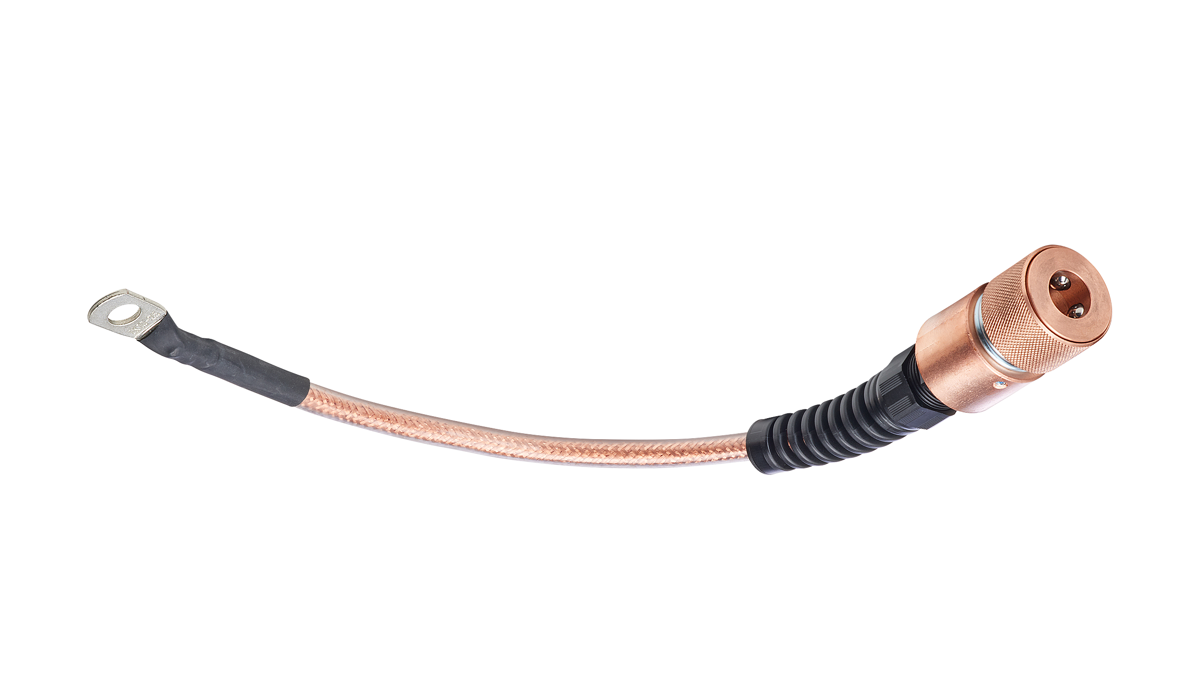
Grounding planes, often referred to as ground planes, serve as the primary reference point for electrical circuits, providing a low-impedance path to return current and a stable common voltage. In electrical safety, they are essential for minimizing electromagnetic interference, preventing ground loops, and ensuring that fault currents are safely diverted to earth, thereby protecting both sensitive components and human operators from hazardous potential differences.
The Role of Grounding Planes in Modern Circuitry
At its core, a grounding plane is a large, conductive surface—usually a solid layer of copper on a printed circuit board (PCB)—that acts as the zero-volt reference for the entire system. While many associate grounding purely with physical safety or lightning protection, in electronic architecture, the grounding plane performs a critical safety function: it minimizes the impedance between components.
When currents flow through a circuit, they take the path of least resistance. If a system lacks a robust, continuous grounding plane, these return currents may wander through unintended traces, creating noise, crosstalk, and, in severe cases, dangerous voltage gradients across the board. By providing a low-impedance path, the plane ensures that return currents stay close to the signal traces, reducing the loop area and preventing the circuit from radiating or receiving unwanted electromagnetic energy that could compromise system stability or trigger safety-critical failures.
Electrical Safety vs. Electromagnetic Compatibility
It is vital to distinguish between two distinct but related concepts: safety grounding and signal integrity grounding.
Safety grounding (often mandated by the National Electrical Code or international standards like IEC 60950) is concerned with protecting humans and infrastructure from electric shock. It involves connecting the conductive enclosures of equipment to the earth. In contrast, signal grounding—the domain of the grounding plane—is concerned with the circuit's functional stability. However, the two are inextricably linked. If a signal reference plane is poorly designed, it can lead to device instability, which may inadvertently cause a power supply to malfunction, leading to overheating or physical hazards.
The grounding plane acts as an "equipotential" surface. In an ideal environment, every point on a ground plane should exist at the same voltage potential. If a PCB has a broken or fragmented ground plane, the resistance across the board increases. This creates a "voltage drop" across the ground layer itself, meaning one section of the board might be at 0.1V while another is at 0.5V. This differential, even when small, can cause logic errors in sensitive digital sensors—a major concern in medical, automotive, or industrial control systems where such errors could lead to dangerous operational outcomes.

Anatomy of an Effective Grounding Plane
To function effectively, a grounding plane must be continuous. The most common mistakes in board design involve "slitting" or "splitting" the plane to separate digital and analog signals. While this is sometimes done to isolate high-frequency noise, it often creates unintended safety hazards if the return currents are forced to take a circuitous path, increasing impedance and radiation.
Best Practices for PCB Ground Plane Design
- Solid Continuity: Use a solid, uninterrupted copper plane whenever possible. Avoid placing signal traces that create "islands" or "slots" in the ground plane.
- Short Return Paths: Always ensure that components are as close to the grounding plane as possible through low-inductance vias.
- Current Density Management: In high-power applications, ensure the copper thickness (often measured in ounces per square foot) is sufficient to handle expected currents without excessive heating.
- Decoupling Integration: The grounding plane works in tandem with decoupling capacitors. These capacitors must be placed as close as possible to the power pins of integrated circuits, with the other end connected directly to the ground plane to suppress transient spikes that could lead to arcing or component breakdown.
Comparing Grounding Strategies
The choice of grounding strategy depends on the frequency of operation and the power density of the system. The following table compares common grounding methodologies used in modern electronics.
| Strategy | Ideal Use Case | Safety Implications | Complexity |
|---|---|---|---|
| Solid Ground Plane | General purpose, high-speed digital | Highest stability, minimizes voltage drops | Low |
| Star Grounding | Low-frequency analog, precision sensors | Eliminates ground loops, prevents noise coupling | Moderate |
| Split Planes | Mixed-signal (Analog/Digital) | High risk of EMI if signals cross gaps | High |
| Multi-layer Grounding | Complex, high-density PCBs | Excellent distribution, lowers parasitic inductance | High |
Troubleshooting Ground Plane Issues
If a device is exhibiting erratic behavior, the grounding plane is often the first place to investigate. Symptoms of a compromised grounding plane include unexplained software crashes, components running hotter than specified, or excessive heat near signal connectors.
Identifying Hidden Hazards
- Ground Loops: If multiple ground points are connected at different potentials, a current loop is formed. This acts like an antenna, picking up noise and creating heat. You can identify these using an oscilloscope to look for high-frequency hum (typically 60Hz or 50Hz) on the ground plane.
- Via Impedance: If the connection between a chip and the ground plane relies on a single, long via, the inductance of that via can cause significant voltage spikes during high-speed switching. The solution is usually to add multiple, parallel "stitching vias" to reduce the total inductance to ground.
- Trace Heating: In high-current applications, verify that the grounding copper is not necked down (thinned) to pass through a narrow channel. This increases resistance, causing a localized "hot spot" that can melt solder or damage the board substrate over time.
Verification and Testing Methods
In 2026, engineers utilize advanced simulation software (such as SI/PI solvers) to analyze the current density across ground planes before a prototype is even manufactured. However, empirical testing remains the gold standard for safety verification.
Practical Verification Steps
- Low-Resistance Measurement: Using a micro-ohmmeter, measure the resistance between the power supply ground and the most distant ground point on the board. A significant jump in resistance often indicates a narrow or broken connection within the plane.
- Thermal Imaging: Utilize infrared cameras while the device is under full load. A healthy ground plane should distribute heat evenly. Hot streaks or isolated hotspots near traces are indicative of localized resistance due to insufficient copper pour.
- Transient Analysis: Observe the system during power-up. If the ground reference shifts momentarily, it can cause latch-up conditions in CMOS components, potentially leading to permanent device failure.
Regulatory Standards and Compliance
While internal PCB design is often considered an engineering choice, certain industries enforce strict grounding requirements to ensure electrical safety. Organizations such as the Institute of Electrical and Electronics Engineers (IEEE) and the International Electrotechnical Commission (IEC) publish standards regarding Electromagnetic Compatibility (EMC).
For example, in industrial equipment, the grounding plane must not only handle return current but must also be robust enough to survive static discharge (ESD) events. If a user touches a chassis, the ESD path must be safely shunted to the ground plane and subsequently to the earth, rather than passing through sensitive processor pins. Failure to provide this low-impedance path to the chassis ground—which should be tied to the PCB ground plane—can result in catastrophic hardware failure and, in rare instances, electrical fire hazards.
Common Myths and Misconceptions
There is a pervasive myth that "more copper equals better grounding." While surface area is critical, the connectivity of that area is what matters. A large copper pour that is only connected to the main ground at a single point via a thin trace is not a grounding plane; it is an antenna. Effective grounding relies on the strategic placement of vias and the avoidance of "dead zones"—areas of copper that are not electrically connected to the primary ground network. These dead zones should be removed or stitched to the primary plane to prevent them from acting as capacitive couplers for noise.
Future-Proofing Electronic Designs
As we move toward higher-frequency processors and more densely packed electronic systems, the importance of the grounding plane only increases. Designs must account for "skin effect," where high-frequency current travels only on the outer surface of a conductor. In 2026, many designs now utilize buried grounding planes in 6-to-12-layer boards to ensure that high-speed return paths are as short as possible, effectively sandwiching high-speed signal layers between ground planes to shield them from environmental interference and ensure long-term operational safety.
Frequently Asked Questions
1. Can a grounding plane replace a physical earth ground?
No. A grounding plane is for signal reference within a device, whereas earth ground is for safety protection against fault conditions. While the two are usually tied together at a single point (the star point) within a device to ensure an equipotential, they perform different functions and cannot be interchanged.
2. Does every layer of a PCB need a ground plane?
Not necessarily. While multi-layer boards often use a "ground-signal-ground" stack-up for high performance, simple designs can function with a single, well-routed ground plane. The goal is to provide a reference path that is as close to the signal traces as possible, regardless of the board's layer count.
3. What happens if I cross a split in the ground plane with a signal trace?
Crossing a split in the ground plane is one of the most common causes of EMI failure. It forces the return current to take a much larger loop, which increases radiation and impedance, likely leading to signal integrity issues and potential safety-related logic failures.
4. How do I determine the appropriate thickness for a ground plane?
Ground plane thickness is determined by the current density it must carry. For most signal-level electronics, standard 1oz copper is sufficient. For power electronics or high-current systems, 2oz or 3oz copper may be required to maintain low resistance and manage heat dissipation effectively.
5. Is it necessary to use "stitching vias" for ground planes?
Yes, especially in multi-layer boards. Stitching vias connect different layers of ground planes together, keeping the impedance low across the entire stack-up and ensuring that the planes act as a single, unified reference rather than multiple disparate surfaces.
Final Recommendation
When designing or repairing equipment, treat the grounding plane as the most critical component of the assembly. Prioritize a solid, continuous pour over any complex routing schemes. If you are experiencing noise, instability, or overheating, begin your diagnostic process by mapping the ground plane for bottlenecks, long return paths, or unstitched islands. Always ensure that the signal reference ground is tied to the chassis safety ground according to the specific manufacturer's design guidelines for the equipment class.
Image Gallery
Select an image to open it in a new tab.

Ingrid Bjornson
Global Cyber Policy and Regulation Analyst
