Understanding the 555 IC Diagram: Pinout, Schematic Structure, and Circuit Operation

A 555 timer integrated circuit diagram maps out its internal architecture and external pin connections, showing how voltage comparators, flip-flops, and output stages work together to create precise timing pulses, oscillators, and time delays in electronic circuits.
Introduction to the 555 Timer IC
The 555 timer integrated circuit is one of the most versatile and widely used microcircuits in the history of electronics. First introduced by Signetics in 1971 as the SE555/NE555, this robust device remains a staple in educational laboratories, industrial controls, and hobbyist projects. At its core, a 555 IC diagram serves as a roadmap for understanding how the chip controls time, generates frequencies, and switches states. Whether you are building a simple flashing LED circuit, designing a pulse-width modulation controller, or generating clock pulses for digital logic, mastering the 555 IC diagram is an essential foundational skill.
When examining a 555 timer, technicians and engineers typically look at two distinct types of diagrams: the external pinout diagram, which shows how to wire the chip into a printed circuit board or breadboard, and the internal functional block diagram, which reveals the transistors, resistors, comparators, and flip-flops that dictate the chip's internal behavior. Understanding both perspectives allows you to calculate external resistor and capacitor values accurately, troubleshoot faulty circuits, and adapt the timer for astable, monostable, or bistable operation modes.
External Pinout and Physical Configuration
The standard 555 timer IC is most commonly packaged in an 8-pin Dual In-line Package (DIP), though surface-mount technology (SMT) variants also exist. To safely and effectively wire the chip, you must understand the function of each pin. Pin numbering begins at the top-left notch or dot, proceeding counter-clockwise down the left side (Pins 1 through 4) and continuing up the right side (Pins 5 through 8).
- Pin 1: GND (-), Pin 8: VCC (+)
- Pin 2: Trigger, Pin 7: Discharge
- Pin 3: Output, Pin 6: Threshold
- Pin 4: Reset, Pin 5: Control Voltage
Each pin plays a specific role in managing voltage thresholds and external timing components. Reviewing these pins individually clarifies how external signals interact with the internal circuitry:
- Pin 1: Ground (GND): Connected to the negative power supply rail or ground reference of the circuit.
- Pin 2: Trigger (TRIG): An input monitoring a voltage drop. When the voltage on this pin falls below one-third of the supply voltage ($V_{CC}$), it sets the internal flip-flop and forces the output high.
- Pin 3: Output (OUT): The primary output terminal of the chip. It can source or sink up to 200 milliamperes of current, making it capable of driving LEDs, small relays, and logic gates directly.
- Pin 4: Reset (RESET): An active-low input used to interrupt timing cycles or force the output low. When pulled below approximately 0.7 volts, the timer resets immediately. In circuits where reset functionality is not needed, this pin is typically tied directly to $V_{CC}$ to prevent accidental triggering.
- Pin 5: Control Voltage (CV): Allows external access to the internal voltage divider node, which sits at two-thirds of $V_{CC}$. Applying an external voltage here alters the internal comparison thresholds, enabling modulation of timing intervals or pulse widths. When unused, it is standard practice to connect a 10-nanofarad capacitor from this pin to ground to filter out electrical noise.
- Pin 6: Threshold (THRES): An input monitoring voltage rises. When the voltage on this pin exceeds two-thirds of $V_{CC}$, it resets the internal flip-flop and drives the output low, provided the trigger condition is not active.
- Pin 7: Discharge (DISCH): An open-collector output connected to an internal transistor. It synchronizes with the output state, discharging the external timing capacitor to ground when the output goes low.
- Pin 8: Power Supply ($V_{CC}$ / $V_{DD}$): The positive supply voltage pin. Standard bipolar 555 timers generally operate across a voltage range of 4.5 volts to 16 volts direct current, while complementary metal-oxide-semiconductor (CMOS) variants such as the ICM7555 can operate at lower voltages.

Internal Functional Block Diagram
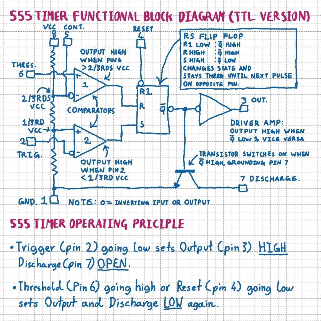
To fully comprehend why the 555 timer behaves the way it does, one must examine its internal schematic. Inside the silicon die, the chip relies on a network of approximately 25 transistors, 2 diodes, and 15 resistors. The functional block diagram breaks this complex arrangement down into four primary subsystems: a resistive voltage divider, two analog comparators, an SR (Set-Reset) flip-flop, and an output buffer stage with a discharge transistor.
The Voltage Divider Network
Connected directly between $V_{CC}$ (Pin 8) and Ground (Pin 1) is a series string of three identical 5-kilohm resistors. This simple divider creates two precise reference voltage points:
- Two-thirds ($2/3$) of $V_{CC}$ at the junction feeding the threshold comparator.
- One-third ($1/3$) of $V_{CC}$ at the junction feeding the trigger comparator.
The Comparators
Two operational amplifiers configured as voltage comparators monitor the external trigger and threshold pins against the internal reference voltages established by the divider string:
- Trigger Comparator: Its non-inverting input connects to Pin 2 (Trigger), while its inverting input connects to the $1/3$ $V_{CC}$ reference. When the trigger voltage drops below $1/3$ $V_{CC}$, this comparator triggers the set input of the flip-flop.
- Threshold Comparator: Its inverting input connects to Pin 6 (Threshold), while its non-inverting input connects to the $2/3$ $V_{CC}$ reference. When the threshold voltage rises above $2/3$ $V_{CC}$, this comparator triggers the reset input of the flip-flop.
The SR Flip-Flop and Output Stage
The SR flip-flop acts as the memory element of the 555 timer, holding the current state of the circuit until instructed to change by one of the comparators. When the trigger comparator fires, the flip-flop sets, driving the output high through an amplification buffer stage and turning off the discharge transistor. Conversely, when the threshold comparator fires, the flip-flop resets, driving the output low and turning on the discharge transistor to drain the timing capacitor.
555 Timer Operating Modes Visualized
The versatility of the 555 timer stems from how external resistors and capacitors are wired around its core pins. Depending on the configuration chosen, the circuit diagram shifts to support one of three primary operational modes.
1. Monostable Mode (One-Shot)
In monostable mode, the 555 IC acts as a precision timing delay generator. When an external trigger pulse pulls Pin 2 below $1/3$ $V_{CC}$, the output switches high for a predetermined duration determined by the formula:
$$T = 1.1 \times R \times C$$
Where $T$ is the time in seconds, $R$ is the external resistance in ohms, and $C$ is the external capacitance in farads. Once the capacitor charges up to $2/3$ $V_{CC}$, the threshold comparator trips, ending the pulse and returning the output to a low state. This configuration is widely used in touch switches, missing pulse detectors, and timer-controlled relays.
2. Astable Mode (Free-Running Oscillator)
When wired in astable mode, the 555 timer operates as a continuous pulse generator or square-wave oscillator. The circuit does not require external triggering; instead, it continuously charges and discharges a capacitor through a pair of resistors ($R_1$ and $R_2$).
- Charging Time ($T_1$): Controlled by $(R_1 + R_2) \times C \times 0.693$
- Discharging Time ($T_2$): Controlled by $R_2 \times C \times 0.693$
- Total Period ($T$): $T_1 + T_2$
- Frequency ($f$): $1 / T$
This mode is essential for generating clock signals, audio tone generators, flashing LED circuits, and pulse-width modulation drivers for direct current motor speed control.
3. Bistable Mode (Flip-Flop)
In bistable mode, the 555 circuit behaves like a basic memory switch or toggle switch. The threshold pin is grounded, and the trigger and reset pins are pulled high using pull-up resistors. Pressing a button connected to the trigger pin forces the output high, where it remains indefinitely until a separate button pulse pulls the reset pin low. This mode requires no external timing capacitors.
| Operating Mode | Primary Function | Key External Components | Typical Applications |
|---|---|---|---|
| Monostable | Single pulse generator / Time delay | One resistor, one capacitor | Timed relays, touch switches, alarms |
| Astable | Continuous square wave / Oscillator | Two resistors, one capacitor | Clock generators, LED flashers, sirens |
| Bistable | Static memory switch | Pull-up resistors, push buttons | Toggle switches, latching circuits |
Step-by-Step Circuit Verification and Troubleshooting
Working with physical 555 timer circuits requires methodical verification to ensure components match the theoretical diagram. Because minor wiring errors can prevent oscillation or lock the output in a static state, following a structured troubleshooting sequence saves time and prevents component damage.
- Check Power Supply Rails: Verify that Pin 8 receives the correct positive voltage and Pin 1 connects securely to ground. Use a digital multimeter to confirm that voltage is present directly at the IC pins, not just at the power supply terminals.
- Inspect the Reset Pin: Ensure Pin 4 is not left floating. If left unconnected, stray electromagnetic interference can cause random, intermittent circuit resets. Tie it to $V_{CC}$ unless an active reset button is explicitly required.
- Verify Control Voltage Filtering: Confirm that Pin 5 has a small decoupling capacitor (typically 10 nF) tied to ground if operating in noisy electrical environments.
- Calculate Component Tolerances: Double-check your resistor and capacitor values against your target timing equations. Ensure electrolytic capacitors are inserted with correct polarity orientation.
- Test Output Drive Limits: Remember that standard bipolar 555 timers can source or sink up to 200 mA. If your load requires higher current—such as high-power automotive lamps or inductive motor loads—interface the 555 output through a power transistor, MOSFET, or optocoupler, and include a flyback diode across inductive loads to prevent voltage spikes.
Frequently Asked Questions
What is the difference between a bipolar 555 and a CMOS 555 IC diagram?
While both share identical pinout configurations and logical functions, internal schematics differ significantly. Bipolar versions (like the classic NE555) use standard transistors and draw higher quiescent current. CMOS versions (like the ICM7555) use field-effect transistors, resulting in significantly lower power consumption, higher input impedance, and the ability to operate at much lower supply voltages and frequencies.
Can a 555 timer produce a true 50% duty cycle in astable mode?
In a standard astable circuit configuration, the charging path includes both $R_1$ and $R_2$, while the discharging path includes only $R_2$. This makes a true 50% duty cycle mathematically impossible because the charging time is always slightly longer than the discharge time. To achieve a 50% duty cycle, engineers modify the standard diagram by adding a fast-switching diode across resistor $R_2$, allowing the capacitor to bypass $R_2$ during the charging cycle.
Why is Pin 5 called Control Voltage if it is often left unconnected?
Pin 5 provides direct physical access to the internal voltage divider node that sets the $2/3$ $V_{CC}$ threshold. While it is frequently left unconnected in basic timing circuits, advanced designers use it to inject external analog voltages. This modulates the internal comparison threshold, allowing the output pulse width or oscillation frequency to be controlled by an external sensor or audio signal.
What causes a 555 timer output to oscillate rapidly or lock up?
Output lockup or erratic oscillation is usually caused by power supply noise, missing decoupling capacitors, or floating control pins. Because the internal switching stages draw brief current surges during state transitions, placing a 0.1-microfarad ceramic capacitor directly across the $V_{CC}$ and ground pins as close to the IC as possible is standard engineering practice to stabilize the internal supply rails.
Conclusion
Analyzing a 555 timer IC diagram bridges the gap between theoretical electronics and practical hardware design. By breaking down the device into its external pin layout, internal comparator blocks, and fundamental operating modes, you gain complete control over how the circuit manages time and frequency. Whether you are constructing an astable clock oscillator for a digital project or designing a monostable delay circuit for industrial automation, careful attention to schematic connections, component sizing, and power supply decoupling ensures reliable performance across every application.
Image Gallery
Select an image to open it in a new tab.


Simon Caldwell
Enterprise Technology and Systems Editor
